Transistors have revolutionised the world in ways people of our age can’t fully comprehend. From shrinking computers the size of rooms to the size of our palms to electronizing every piece of technological equipment we come across these days. But the era of silicon based transistors is slowly coming to an end.
Moore’s law is the observation that the number of transistors in a dense integrated circuit doubles about every two years. This directly translates to the fact that size of the transistor decreases every two years. The size of a transistor can’t indefinitely keep decreasing, the size of a transistor in a modern day chip is about 7-14nm. That’s incredible! It means that there are around 6.5 billion transistors on a single chip that’s the size of your thumbnail. But we can’t indefinitely go on decreasing the length of a transistor because quantum effects such as quantum tunneling begin to take place which results in the transistor being in the on state even if it is off. So what’s the solution?
In the not so distant past a wonder material was discovered with applicational possibilities that belittle the silicon transistor. So what is this wonder material? It’s a carbon based material made of a single layer of carbon atoms, it’s 200 times stronger than steel and 6 times as light. It’s graphene.
PROPERTIES
Some of the properties for an ideal transistor would be sufficiently
1)wide band gap, high thermal conductivity.
2)producible on large diameter substrates.
3)interfaces with dielectrics with lasting stability.
4)Low contact resistance.
Natural large area graphene behaves like a semi-metal because it is gapless and hence the first condition is already fulfilled. Graphenes band structure structure differs from silicons, the valence and conduction band meet due to which it is gapless in nature.

Due to a missing band gap graphene MOSFETs do not switch off. This problem is overcome by introducing a band gap by forming graphene nanoribbons(GNR).
Gapless large area graphene shows high mobilities. The mobility depends on carrier concentration. Most semiconductors these days are rigid and not useful in the emerging fields of flexible electronics in contrast large area graphene is bendable and recent advances in graphene technology show uses of graphene ink for printed electronics. Graphene opens the door to high-frequency low-voltage flexible and printable electronic applications.
PRINCIPLE OF WORKING
Coming to the icing of the cake. AIST(Advanced Industrial Science and Technology) have developed a graphene transistor with a new operating principle.
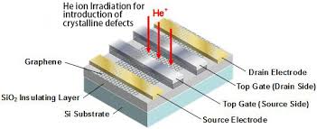
In the newly developed transistor there are two electrodes and two top gates namely source and drain on the graphene and the graphene between the top gates is irradiated with helium ion beam to introduce crystalline defects. Gate biases are applied to the two top gates independently, allowing carrier densities in the top gated graphene region to be controlled. The transistor polarity can be controlled and inverted, which to date has not been possible for transistors.
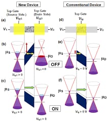
The operating principle of the new transistor is shown in figure below.
In order to create a transport gap in graphene of the channel between the two gates was irradiated with helium ions to introduce crystalline defects that create a band gap. The energy band of the graphene on both sides can be controlled by applying biases to the top gates. The polarity of the carriers in graphene can be changed between n and p type based on the polarity of the biases on the top gates. When polarities differ the transistor is in the off state, carrier transport is blocked by a barrier formed in the transport gap. In the developed transistor the channel length can be made smaller than that of a conventional transistor. Since these transistors achieve a better off state with small transport gap the channel length can be reduced compared to conventional transistors allowing it to have faster on/off operations.
APPLICATIONS
Sky’s the limit as they say. Graphene transistors can be used to create transparent memory. Rice University researchers have succeeded in developing transparent flexible memory chips using silicon oxide as the active component. Better faster and smaller integrated circuits can be developed. IBM has developed graphene transistors and it’s proven to be twice as fast as silicon transistors.
Steering away from transistors, Chinese researchers have developed a battery foam transistor design that can bridge the gap between batteries and capacitors. It can discharge and charge as quickly as a capacitor and can discharge completely in 20 seconds. It is also flexible, and works even when it is bent.
Graphene has been developed for touch screen displays too. Graphene film is a strong candidate for the replacement of indium tin oxide. It can be used in touch screens on table computers and smartphones and can also be used as an electrode in solar cells and OLEDs. Graphene film is much stronger and can withstand falls even at large heights.
CONCLUSION
The applications of graphene are limitless. If there’s anything that could possibly change the way we look and use tech, it’s graphene. Humanity has come a long way from the wheel and we’ve yet to traverse the vast expanse of possibilities and infinite of tomorrow. Graphene amongst it’s elder siblings of silicon and the likes are merely the founding stones for something bigger. So with our eyes trained on the future and minds learning from the past and hearts focused on helping the people, lets create a better tomorrow.
– Abhinav Pavithran